Power supply on carrier
This article is about designing the power supply on the carrier board. The purpose is to share some of our experiences and give an introduction to the subject.The power supply circuitry typically is based on a combination of linear and switching voltage regulators. The former is uncomplicated and inexpensive but inefficient. The latter saves power but is somewhat challenging to the designer and costs more. Embedded design based on a COM Module and a carrier board is often a cost-effective strategy. The COM module is a COTS product, verified and ready to be used in the design. Thus complications involved in hardware design involving processor and chipset are not your headache.
The challenges are limited to the carrier board where functions, components and interfaces needed for your specific application are placed. An embedded design based on a COM module and a carrier board allows you to stay focused on your core competence.
A common strategy is to use the 12V or 24V supply that often is at hand and use regulators on the carrier board to feed proper voltage levels to components on the carrier board including the COM module.
The COM module internally uses five or six different voltage levels down to sub 1V. The power regulators on the module are in some cases developed specifically for each new processor generation and include functionality closely connected to the processor working modes. The design is complex and the documentation is typically protected.
But then again, you chose a semi-custom design to avoid these difficulties. Carrier boards usually make do with two or three voltage levels. 5V, 3,3V and 1,8V are required in the example we are going to discuss. |
|
|
|
|
Selecting voltage regulator type |
|
|
Let’s make some initial calculations based on the Hectronic H6049 Qseven module only. It uses 5V and consumes a maximum of 1A. There are a couple of techniques to decrease, let’s say 12V, to the required 5V voltage. An uncomplicated design uses a linear voltage regulator. The regulator merely requires a couple of resistors and capacitors typically. Input is 1A at 12V and output is 1A at 5V. Thus the input power is 12W and the output power 5W. The drawback is the 7W power loss. The linear voltage regulator is inexpensive, uncomplicated and stable, but not good enough, at least not in this case.
The switching voltage regulator is the better choice. Power loss is typically under 10%. Let’s say that the carrier board is equipped with the H6049 Qseven module and a couple of USB interfaces that require 5V power. The module consumes 1A and the USB ports 0,5A each. It’s likely to be the major power load of the design. It’s worth while to put the effort into using a switching regulator for the 5V supply. A decreased power loss is what we’re after. |
|
|
|
|
Getting an overview – The power budget |
|
|
Let’s make a simple power budget in order to get an overview of power consumptions and voltage levels for the components included on the carrier board. It helps in the decision upon a suitable combination of linear and switching regulators. A detailed power budget includes consumptions for various working modes (full, idle, sleep etc). Our budget focuses on maximum figures added separately for components at each voltage level.
|
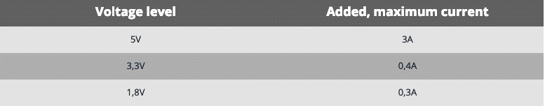
Picture 1: Table of voltage levels and currents
|
Large currents and a big gaps between input and output voltage lead to large power loss using a linear regulator. The simplicity of the design doesn’t compensate for the inefficiency. It’s another thing when loads are lighter. It means that the power losses are smaller and heat dissipated is not a problem using a linear voltage regulator.
|
|
|
|
|
A combination of switching and linear regulators |
|
|
In this case I would suggest to use a switching voltage regulator to feed the carrier board 5V with enough capabilities for all parts and components of the design. Thereafter step down from 5V to 3,3V and 1,8, either directly to each separate voltage level or from 5V to 3,3V and from 3,3V to 1,8V using linear regulators. In this case we decide to choose the former strategy. Let’s calculate the power loss of the design to determine if it’s acceptable or not.
The calculations are performed on each separate regulator. The first one out is the switching regulator. The output current is the sum of all three currents; at the 5V voltage level, at 3,3V and 1,8V. |
|
|
|
|
Switching voltage regulator |
|
|
Uin = 12V Uout = 5V Iout = (3+0,4+0,3)A = 3,7A
The power loss is determined as follows and is based on the assumption that the power loss in the regulator is 10%. In other words 90% of the power is distributed efficiently through the circuit.
(12V x IinA) x 0,9 = 5V x 3,7A
Iin = (5V x 3,7A) / (12V x 0,9) = 1,71A
The power loss is the difference between the input power and the output power.
Pin = 12V x 1,71A = 20,5W
Pout = 5V x 3,7A = 18,5W
Ploss = Pin – Pout = 20,5W – 18,5W = 2W
The power losses from the two additional linear voltage regulators are calculated using similar principals. |
|
|
|
|
3,3V linear voltage regulator |
|
|
|
|
|
Uin = 5V Uout = 3,3V Iin = Iout = 0,4A
Pin = 5V x 0,4A = 2,0W
Pout = 3,3 x 0,4A = 1,3W
Ploss = Pin – Pout = 2,0W – 1,3W = 0,7W
|
|
1,8V linear voltage regulator |
|
|
|
|
|
Uin = 5V Uout = 1,8V Iin = Iout = 0,3A
Pin = 5V x 0,3A = 1,5W
Pout = 1,8 x 0,3A = 0,5W
Ploss = Pin – Pout = 1,5W – 0,5W = 1,0W |
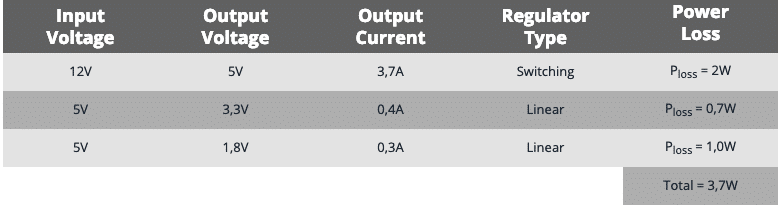
Picture 2: Power budget
|
The total power loss from such a power design is 3,7W. If it’s acceptable then it’s time to proceed to the next phase. If not, an option is to change from linear to switching technology for one or both of the lower voltage levels. The 1,8V voltage level has priority since it introduces the bigger power loss of the two, therefore presents the greater potential of improvement. Let’s say that the power loss levels are acceptable. |
|
|
|
|
Switching regulators – Components and component values |
|
|
Components necessary for switching regulators vary. Some regulator models need two transistors and a coil, some a transistor, a diode and a coil and yet other switching regulators have the compulsory coil integrated. They all need some capacitors and most of them also a couple of resistors to be added to the design. Generally speaking the larger the degree of integration the less complications to the design work.
|
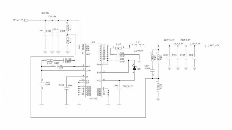
Picture 3a: Example of a switching voltage regulator – Schematics
Tool support in design work |
|
Designing a power supply using switching regulators has been rather complicated until recent years. Nowadays the tools made available by suppliers have made selection of components and calculation of component values significantly easier. Data such as input voltage, output voltage, output current and a couple of answers to stated questions will allow the tool to suggest components and component values in order to accomplish a stable design that meets the requirements.
In some cases it’s even possible for the designer to state preferred components and have the tool suggest the rest of the components and component values to meet requirements. Warnings about too much heat or instability in the design are issued by the tool.
As the switching voltage regulator design is completed we have addressed the more complicated part of the work. The linear voltage regulators are reasonably uncomplicated to use. Picture 4a and 4b show an example. |
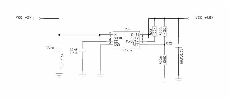
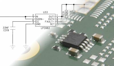
Picture 4a: Example of a linear voltage regulator – Schematics
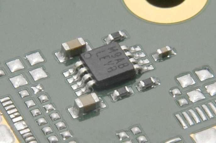
Picture 4b: Example of a linear voltage regulator – Components on carrier board
|
Voltage drop is an issue when selecting the linear voltage regulator to use. A small gap between input and output voltage limits the number of regulators possible to use. In that case, look for LDO, Low-Dropout versions of regulators.
|
|
|
|
|
Linear regulators – Components and component values |
|
|
Selection of components and component values for the required resistors and capacitors is fairly uncomplicated. No tools are required. Just rely on formulas, tables, suggestions and reference designs at hand on supplier websites.
A general strategy at Hectronic is to reuse building blocks. I have a library of well-tried circuit designs using linear and switching technology, one or two for applications that require large currents and low currents respectively. A regulator with an adjustable output voltage is advantageous. The voltage level is adjusted to the requirements at hand merely by changing a couple of resistors. Thereby it’s possible to reuse a trusted and familiar design one time after another.
I hope that I have shed some light upon how to design the power supply on your carrier board. The task may seem challenging but mustn’t be. The development during recent years include software tools and highly integrated regulators to make things easier. The more complicated power supply functionality is included on the COM module enabling designers using the semi-custom design to focus their efforts on functionality crucial to the final product and the requirements from their customers. |